SPI Interface Big 7-Seg LED


The circuit uses a serial-in-parallel out shift register, 74HC595 for receiving serial data from uController board. See example of U5 in the schematic, SER is for data input, SRCLK is shift clock and RCLK is Latch clock. Each data bit is shifted into the register on rising edge of the shift clock. When all data bits are shifted into the 8-bit register, the rising edge of RCLK will clock the data to be latched at each output bit, i.e. QA - QH.

The Big LED is made from cheap dot LED. Each segment has five dot LED connected in series with a limiting resistor tied to +12V. The logic high at the input of ULN2003 makes the output active low, thus sinks the LED current into the chip. The driver has 7-bit for segment a, b, c, d, e, f, and g. Q1 is for optional point display.

Multiple digits can easily be made by connecting the QH to the next digit serial input bit, see the circuit below. Please note that, the shift clock and latch signal are

tied to every 74HC595.

Below is exemplary display board with four digits LED for temperature displaying. The control board may be attached to the display board by 10-pin header J2, on the back panel, say.

Digital code lock


This is a simple but effective code lock circuit that has an automatic reset facility. The circuit is made around the dual flip-flop IC CD4013.Two CD 4013 ICs are used here. Push button switches are used for entering the code number. One side of all the push button switches are connected to +12V DC. The remaining end of push buttons 2,3,6,8 is connected to clock input pins of the filp-flops. The remaining end of other push button switches are shorted and connected to the set pin of the filp-flops.
The relay coil will be activated only if the code is entered in correct sequence and if there is any variation, the lock will be resetted. Here is correct code is 2368.When you press 2 the first flip flop(IC1a) will be triggered and the value at the data in (pin9) will be transferred to the Q output (pin13).Since pin 9 is grounded the value is “0” and so the pin 13 becomes low. For the subsequent pressing of the remaining code digits in the correct sequence the “0” will reach the Q output (pin1) of the last flip flop (IC2b).This makes the transistor ON and the relay is energised.The automatic reset facility is achieved by the resistor R11 and capacitor C2.The positive end of capacitor C2 is connected to the set pin of the filp-flops.When the transistor is switched ON, the capacitor C2 begins to charge and when the voltage across it becomes sufficient the flip-flops are resetted. This makes the lock open for a fixed amount of time and then it locks automatically. The time delay can be adjusted by varying the values of R11 and C2.

Notes.

  • Assemble the circuit on a good quality PCB.
  • The circuit can be powered from 12V DC.
  • Mount the ICs on holders.
  • The L1 can be a 12V, 200 Ohm SPDT relay.
  • Capacitor C1 should be tantalum type.
  • The C1 and C2 must be rated at least 25V.

LM555 Voltage Doubler


This circuit shows the voltage doubler working with a 555. LM555 has good drive 200mA, both Vcc and Gnd.

TV remote control Blocker


Just point this small device at the TV and the remote gets jammed . The circuit is self explanatory . 555 is wired as an astable multivibrator for a frequency of nearly 38 kHz. This is the frequency at which most of the modern TVs receive the IR beam . The transistor acts as a current source supplying roughly 25mA to the infra red LEDs. To increase the range of the circuit simply decrease the value of the 180 ohm resistor to not less than 100 ohm.

It is required to adjust the 10K potentiometer while pointing the device at your TV to block the IR rays from the remote. This can be done by trial and error until the remote no longer responds.

Battery Tester Project Using LM3914 IC


This objective of this project is to design and build a battery tester that is able to test various types of dry cell and rechargable battery with a voltage of less than 2V. Configured as a bar graph battery level indicator, the LM3914 IC from National Semiconductor senses the voltage levels of the battery under test and drives the 10 LEDs to ON or OFF based on the voltage that is detected. The current driving the LEDs is regulated by using the external resistor R1 and hence limiting resistors are not required.

The schematic shows the simple connections where the reference voltage at pin 8 of U1 can be adjusted by adjusting the variable resistor VR1. The voltage at pin 8 will set the maximum scale of the LED. In testing dry cell battery of 1.5V, set the voltage at pin 8 to 2.0V. Each of the LED will thus represent 200mV when lighted up.

If testing of rechargable battery such as NiCd or NiMH is required, set the reference voltage to a lower value such as 1.5V as the typical voltage of a rechargable battery is approximately 1.2V.

When testing the battery, take note of the polarity of the probe to the terminals of the battery. T1 is to be placed on the positive terminal and T2 the negative terminal of the battery.

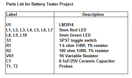
Parts List

The parts list of the project is as shown below.

SOLAR REVOLVER


How would you use an SE with a chip enable? Good question and well one thing leads to another and before you know it a new solar roller is born. The design started out as a simple example of using the 1381wr SE to enable a 74AC240 chip. But with all those spare inverters looking for something to do, the SE kind of got integrated with a whole new solar roller design. The Solar Revolver v3 is the latest incarnation of an evolving circuit. If you have followed the design so far, you will agree that first two versions looked pretty on paper but they had less than stellar performance in reality. They were not very efficient during direction changes and had unpredictable behavior.

The Solar Revolverv3 is recommend for those who would like to test out this single chip solar roller with turn and reverse which has some unique features and is very efficient.

- 1. new 1381 SE with timed reset
- 2. revolve (turn) left/right
- 3. reverse
- 4. new ultra low power delay Nu
- 5. new delay Nu memory

NEW 1381 SE

The original intention was to use a variation of the 1381wr SE to enable a 74AC240 chip, but that SE is designed to drive a motor directly and would be overkill. The simple Miller Engine would suitable but I opted for a new 1381 SE design in the Solar Revolver v3 which also uses a timed reset and uses the same number of parts but has a higher trigger voltage: the 1381tr SE .

As shown, this SE uses a 1381E voltage detector with a red LED in series to raise the trigger level to 4.0V. A 10uF cap between the 1381 power and ground pins together with the 1M resistor on the output pin causes the SE to reset after about 1 second. A single NPN transistor used used as a inverter to match the requirement for a low current active low enable. For this application , the 1381tr SE works just like the Miller Engine and draws less than a uA of current during charging.

I used a Sunceram 5V solar cell and and 10,000 uF cap (C1) to match the SE 4V trigger voltage. The C1 cap can be any value between 10,000 uF to 1F . Since the length of time that the SE is active is primarily determined by the SE capacitor it means that small capacitor values for C1 give deep discharges and large C1 caps would hold up the voltage during discharge to give quicker charging times. With a large C1 and a change in the SE cap the motors can run for a lot longer than 10 seconds but also take longer to charge back up.

When the 1381 output goes high it drives the 2N3904 inverter base through the 1M resistor and the active low collector signal is used to control the enable pin 19 of the four inverters of group B.

Two inverters of group A and two inverters of group B are used to drive the motors and when inverters B are disabled motor drive is turned off (High-Z) and the motors continue to "freewheel" while power consumption drops to zero.

NEW TURN DELAY CIRCUIT

The left/right turn and reverse switches discharge the 10uF delay caps and reverse one or both motors. This causes the roller to revolve around its center or to back up. The turn/reverse time is about 4 seconds BUT the delay only times out when the SE is active. If the SE is active for 1 second it will take 4 or 5 bursts of motion for the delay to time out. In fact, depending on the charging time, the 4 second turn or reverse period can take much longer and be spread over minutes of charging interspersed with short bursts of motion.

A second inverter from group A is used with a diode to provide feedback and a transition by rapidly charging up the 10uF caps when the turn and reverse delay Nu times out. This method avoid high frequency oscillation, hesitation and wasted energy during changes in direction.

While the SE is charging, the 10uF capacitors of the turn reverse delay circuit are isolated with the two group B inverter outputs tristated. With the cap essentially disconnected, the inputs to the motor driver are pulled up through the 330K resistors to V+ and CMOS power consumption is zero.

The effect of analog voltages applied to CMOS inputs are a common problem in many solar designs that use RC delay circuits especially when Vcc is above 3V. The analog levels cause high power consumption and oscillations. Analog voltages on a timing capacitor connected to the CMOS input can cause a 74AC240 to draw up to 50ma while charging which would at the very least slow the charging rate and might just hang the circuit up! The new isolating Nu delay circuit is a big improvement over previous designs and avoids all of those problems.

SUMMARY

With the 4V 1381tr Solar Engine, the single 74AC240 design is good enough to drive 2 small efficient motors mounted on a light wheeled platform. The solar powered design includes turn and reverse for two motors and incorporates a new energy saving turn and reverse delay circuit.