SPI Interface Big 7-Seg LED


The circuit uses a serial-in-parallel out shift register, 74HC595 for receiving serial data from uController board. See example of U5 in the schematic, SER is for data input, SRCLK is shift clock and RCLK is Latch clock. Each data bit is shifted into the register on rising edge of the shift clock. When all data bits are shifted into the 8-bit register, the rising edge of RCLK will clock the data to be latched at each output bit, i.e. QA - QH.

The Big LED is made from cheap dot LED. Each segment has five dot LED connected in series with a limiting resistor tied to +12V. The logic high at the input of ULN2003 makes the output active low, thus sinks the LED current into the chip. The driver has 7-bit for segment a, b, c, d, e, f, and g. Q1 is for optional point display.

Multiple digits can easily be made by connecting the QH to the next digit serial input bit, see the circuit below. Please note that, the shift clock and latch signal are

tied to every 74HC595.

Below is exemplary display board with four digits LED for temperature displaying. The control board may be attached to the display board by 10-pin header J2, on the back panel, say.

Digital code lock


This is a simple but effective code lock circuit that has an automatic reset facility. The circuit is made around the dual flip-flop IC CD4013.Two CD 4013 ICs are used here. Push button switches are used for entering the code number. One side of all the push button switches are connected to +12V DC. The remaining end of push buttons 2,3,6,8 is connected to clock input pins of the filp-flops. The remaining end of other push button switches are shorted and connected to the set pin of the filp-flops.
The relay coil will be activated only if the code is entered in correct sequence and if there is any variation, the lock will be resetted. Here is correct code is 2368.When you press 2 the first flip flop(IC1a) will be triggered and the value at the data in (pin9) will be transferred to the Q output (pin13).Since pin 9 is grounded the value is “0” and so the pin 13 becomes low. For the subsequent pressing of the remaining code digits in the correct sequence the “0” will reach the Q output (pin1) of the last flip flop (IC2b).This makes the transistor ON and the relay is energised.The automatic reset facility is achieved by the resistor R11 and capacitor C2.The positive end of capacitor C2 is connected to the set pin of the filp-flops.When the transistor is switched ON, the capacitor C2 begins to charge and when the voltage across it becomes sufficient the flip-flops are resetted. This makes the lock open for a fixed amount of time and then it locks automatically. The time delay can be adjusted by varying the values of R11 and C2.

Notes.

  • Assemble the circuit on a good quality PCB.
  • The circuit can be powered from 12V DC.
  • Mount the ICs on holders.
  • The L1 can be a 12V, 200 Ohm SPDT relay.
  • Capacitor C1 should be tantalum type.
  • The C1 and C2 must be rated at least 25V.

LM555 Voltage Doubler


This circuit shows the voltage doubler working with a 555. LM555 has good drive 200mA, both Vcc and Gnd.

TV remote control Blocker


Just point this small device at the TV and the remote gets jammed . The circuit is self explanatory . 555 is wired as an astable multivibrator for a frequency of nearly 38 kHz. This is the frequency at which most of the modern TVs receive the IR beam . The transistor acts as a current source supplying roughly 25mA to the infra red LEDs. To increase the range of the circuit simply decrease the value of the 180 ohm resistor to not less than 100 ohm.

It is required to adjust the 10K potentiometer while pointing the device at your TV to block the IR rays from the remote. This can be done by trial and error until the remote no longer responds.

Battery Tester Project Using LM3914 IC


This objective of this project is to design and build a battery tester that is able to test various types of dry cell and rechargable battery with a voltage of less than 2V. Configured as a bar graph battery level indicator, the LM3914 IC from National Semiconductor senses the voltage levels of the battery under test and drives the 10 LEDs to ON or OFF based on the voltage that is detected. The current driving the LEDs is regulated by using the external resistor R1 and hence limiting resistors are not required.

The schematic shows the simple connections where the reference voltage at pin 8 of U1 can be adjusted by adjusting the variable resistor VR1. The voltage at pin 8 will set the maximum scale of the LED. In testing dry cell battery of 1.5V, set the voltage at pin 8 to 2.0V. Each of the LED will thus represent 200mV when lighted up.

If testing of rechargable battery such as NiCd or NiMH is required, set the reference voltage to a lower value such as 1.5V as the typical voltage of a rechargable battery is approximately 1.2V.

When testing the battery, take note of the polarity of the probe to the terminals of the battery. T1 is to be placed on the positive terminal and T2 the negative terminal of the battery.

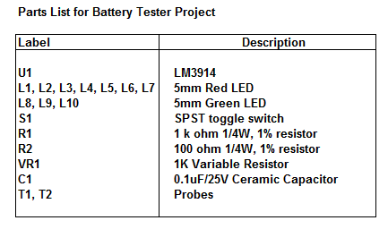
Parts List

The parts list of the project is as shown below.

SOLAR REVOLVER


How would you use an SE with a chip enable? Good question and well one thing leads to another and before you know it a new solar roller is born. The design started out as a simple example of using the 1381wr SE to enable a 74AC240 chip. But with all those spare inverters looking for something to do, the SE kind of got integrated with a whole new solar roller design. The Solar Revolver v3 is the latest incarnation of an evolving circuit. If you have followed the design so far, you will agree that first two versions looked pretty on paper but they had less than stellar performance in reality. They were not very efficient during direction changes and had unpredictable behavior.

The Solar Revolverv3 is recommend for those who would like to test out this single chip solar roller with turn and reverse which has some unique features and is very efficient.

- 1. new 1381 SE with timed reset
- 2. revolve (turn) left/right
- 3. reverse
- 4. new ultra low power delay Nu
- 5. new delay Nu memory

NEW 1381 SE

The original intention was to use a variation of the 1381wr SE to enable a 74AC240 chip, but that SE is designed to drive a motor directly and would be overkill. The simple Miller Engine would suitable but I opted for a new 1381 SE design in the Solar Revolver v3 which also uses a timed reset and uses the same number of parts but has a higher trigger voltage: the 1381tr SE .

As shown, this SE uses a 1381E voltage detector with a red LED in series to raise the trigger level to 4.0V. A 10uF cap between the 1381 power and ground pins together with the 1M resistor on the output pin causes the SE to reset after about 1 second. A single NPN transistor used used as a inverter to match the requirement for a low current active low enable. For this application , the 1381tr SE works just like the Miller Engine and draws less than a uA of current during charging.

I used a Sunceram 5V solar cell and and 10,000 uF cap (C1) to match the SE 4V trigger voltage. The C1 cap can be any value between 10,000 uF to 1F . Since the length of time that the SE is active is primarily determined by the SE capacitor it means that small capacitor values for C1 give deep discharges and large C1 caps would hold up the voltage during discharge to give quicker charging times. With a large C1 and a change in the SE cap the motors can run for a lot longer than 10 seconds but also take longer to charge back up.

When the 1381 output goes high it drives the 2N3904 inverter base through the 1M resistor and the active low collector signal is used to control the enable pin 19 of the four inverters of group B.

Two inverters of group A and two inverters of group B are used to drive the motors and when inverters B are disabled motor drive is turned off (High-Z) and the motors continue to "freewheel" while power consumption drops to zero.

NEW TURN DELAY CIRCUIT

The left/right turn and reverse switches discharge the 10uF delay caps and reverse one or both motors. This causes the roller to revolve around its center or to back up. The turn/reverse time is about 4 seconds BUT the delay only times out when the SE is active. If the SE is active for 1 second it will take 4 or 5 bursts of motion for the delay to time out. In fact, depending on the charging time, the 4 second turn or reverse period can take much longer and be spread over minutes of charging interspersed with short bursts of motion.

A second inverter from group A is used with a diode to provide feedback and a transition by rapidly charging up the 10uF caps when the turn and reverse delay Nu times out. This method avoid high frequency oscillation, hesitation and wasted energy during changes in direction.

While the SE is charging, the 10uF capacitors of the turn reverse delay circuit are isolated with the two group B inverter outputs tristated. With the cap essentially disconnected, the inputs to the motor driver are pulled up through the 330K resistors to V+ and CMOS power consumption is zero.

The effect of analog voltages applied to CMOS inputs are a common problem in many solar designs that use RC delay circuits especially when Vcc is above 3V. The analog levels cause high power consumption and oscillations. Analog voltages on a timing capacitor connected to the CMOS input can cause a 74AC240 to draw up to 50ma while charging which would at the very least slow the charging rate and might just hang the circuit up! The new isolating Nu delay circuit is a big improvement over previous designs and avoids all of those problems.

SUMMARY

With the 4V 1381tr Solar Engine, the single 74AC240 design is good enough to drive 2 small efficient motors mounted on a light wheeled platform. The solar powered design includes turn and reverse for two motors and incorporates a new energy saving turn and reverse delay circuit.

REMOTE-CONTROLLED FAN REGULATOR


Using this circuit, you can change the speed of the fan from your couch or bed. Infrared receiver module TSOP1738 is used to receive the infrared signal transmitted by remote control.
The circuit is powered by regulated 9V. The AC mains is stepped down by transformer X1 to deliver a secondary output of 12V-0-12V. The transformer output is rectified by full-wave
rectifier comprising diodes D1 and D2, filtered by capacitor C9 and regulated by 7809 regulator to provide 9V regulated output.
Any button on the remote can be used for controlling the speed of the fan. Pulses from the IR receiver module are applied as a trigger signal to timer NE555 (IC1) via LED1 and resis-tor R4. IC1 is wired as a monostable multivibrator to delay the clock given to decade counter-cum-driver IC CD4017 (IC2).
Out of the ten outputs of decade counter IC2 (Q0 through Q9), only five (Q0 through Q4) are used to control the fan. Q5 output is not used, while Q6 output is used to reset the counter.
Another NE555 timer (IC3) is also wired as a monostable multivibrator. Combination of one of the resistors R5 through R9 and capacitor C5 controls the pulse width. The output from IC CD4017 (IC2) is applied to resistors R5 through R9. If Q0 is high capacitor C5 is charged through resistor R5, if Q1 is high capacitor C5 is charged through resistor R6, and so on.
Optocoupler MCT2E (IC5) is wired as a zero-crossing detector that supplies trigger pulses to monostablemultivibrator IC3 during zero crossing. Opto-isolator MOC3021 (IC4) drives triac BT136. Resistor R13 (47- ohm) and capacitor C7 (0.01μF) combination is used as snubber network for triac1 (BT136). As the width of the pulse decreases, firing angle of the triac increases and speed of the fan also increases. Thus the speed of the fan increases when we press any button on the remote control.
Assemble the circuit on a generalpurpose PCB and house it in a small case such that the infrared sensor can easily receive the signal from the remote transmitter.

Running Message Display


Light emitting diodes are advan- tageous due to their smaller size, low current consumption and catchy colours they emit. Here is a running message display circuit wherein the letters formed by LED arrangement light up progressively. Once all the letters of the message have been lit up, the circuit gets reset. The circuit is built around Johnson decade counter CD4017BC (IC2). One of the IC CD4017BE’s features is its provision of ten fully decoded outputs, making the IC ideal for use in a whole range of sequencing operations. In the circuit only one of the outputs remains high and the other outputs switch to high state successively on the arrival of each clock pulse. The timer NE555 (IC1) is wired as a 1Hz astable multivibrator which clocks the IC2 for sequencing operations. On reset, output pin 3 goes high and drives transistor T7 to ‘on’ state. The output of transistor T7 is connected to letter ‘W’ of the LED word array (all LEDs of letter array are connected in parallel) and thus letter ‘W’ is illuminated. On arrival of first clock pulse, pin 3 goes low and pin 2 goes high. Transistor T6 conducts and letter ‘E’ lights up. The preceding letter ‘W’ also remains lighted because of forward biasing of transistor T7 via diode D21. In a similar fashion, on the arrival of each successive pulse, the other letters of the display are also illuminated and finally the complete word becomes visible. On the following clock pulse, pin 6 goes to logic 1 and resets the circuit, and the sequence repeats itself. The frequency of sequencing operations is controlled with the help of potmeter VR1.
The display can be fixed on a veroboard of suitable size and connected to ground of a common supply (of 6V to 9V) while the anodes of LEDs are to be connected to emitters of transistors T1 through T7 as shown in the circuit. The above circuit is very versatile and can be wired with a large number of LEDs to make an LED fashion jewellery of any design. With two circuits connected in a similar fashion, multiplexing of LEDs can be done to give a moving display effect

Digital Volume Control & 5 band graphic equalizer

Digital Volume Control

This circuit could be used for replacing your manual volume control in a stereo amplifier. In this circuit, push-to-on switch S1 controls the forward (volume increase) operation of both channels while a similar switch S2 controls reverse (volume decrease) operation of both channels.

A readily available IC from Dallas semiconductor, DS1669 is used here.

FEATURES:

  • Replaces mechanical variable resistors
  • Electronic interface provided for digital as well as manual control
  • Wide differential input voltage range between 4.5 and 8 volts
  • Wiper position is maintained in the absence of power
  • Low-cost alternative to mechanical controls
  • Applications include volume, tone, contrast,brightness, and dimmer control

The circuit is extremely simple and compact requiring very few external components.

The power supply can vary from 4.5V to 8V.

5 band graphic equalizer using a single IC/chip :

This circuit uses a single chip, IC BA3812L for realizing a 5 band graphic equalizer for use in hi-fi audio systems.The BA3812L is a five-point graphic equalizer that has all the required functions integrated onto one IC. The IC is comprised of the five tone control circuits and input and output buffer amplifiers. The BA3812L features low distortion, low noise, and wide dynamic range, and is an ideal choice for Hi-Fi stereo applica-tions. It also has a wide operating voltage range (3.5V to 16V), which means that it can be adapted for use with most types of stereo equipment.

The five center frequencies are independently set using external capacitors, and as the output stage buffer amplifier and tone control section are independent circuits, fine control over a part of the frequency bandwidth is possible, By using two BA3812Ls, it is possible to construct a 10-point graphic equalizer. The amount of boost and cut can be set by external components.

The recommended power supply is 8V, but the circuit should work for a supply of 9V also. The maximum voltage limit is 16V.

The circuit given in the diagram operates around the five frequency bands:

  • 100Hz
  • 300Hz
  • 1kHz
  • 3kHz
  • 10kHz

ANTI-COLLISION REAR LIGHT


During poor visibility, i.e., whenthere is fog, or at dawn or dusk, or when your vehicle gets stalled on a lonely stretch of a highway, this flashing light will provide safety and attract the attention of people to help you out. It uses highbrightness yellow LEDs.
The circuit uses a dual binary counter CD4520, quadruple 2-inputNAND schmitt trigger CD4093, 8-stage shift-and-store bus register CD4094 and some descrete components.
An oscillator is built around gate A, whose frequency can be varied through preset VR1 when required. The output of the oscillator is fed to IC1 and IC3. When the circuit is switched on, the oscillator starts oscillating, the counter starts counting through IC1 and the data is shifted on positive-going clock through IC3. As a result, the four groups of LEDs flash one by one.
All the LEDs will then glow for some time and switch off for some time, and the cycle will repeat. Input pins 12 and 13 of the unused gate D must be tied to ground and pin 11 left open. Preset VR1 should be of cermet type and used to change the flashing rate of each group of LEDs.
The circuit works off regulated 12V. Assemble it on a general-purpose PCB and house suitably.

Staircase Light With Auto Switch-Off


We are all familiar with the electrical wiring arrangement that connects an electrical
bulb with two switches: one at the bottom of a staircase and the other at the top. Wiring is done such that either of the two switches can be used to switch the bulb on or off. In such a wiring arrangement, while climbing up the staircase which is in dark, the switch located at the bottom of the staircase is used to switch on the light. After you have climbed the staircase, you use the switch located there to switch off the light.
The circuit presented here is an electronic-cum-electrical arrangement to get a similar facility as provided by the hard-wired electrical system, but you need to operate the switch only once. Whereas in the hard-wired arrangement if you forget to switch off the light once you have traversed the staircase, light would remain ‘on,’ wasting energy.
In this circuit also, we have two micro-switches—one located at the top and the other located at the bottom of the staircase—that can be pushed and released easily during climb-up from the bottom of the staircase or climbdown from the top of the staircase. With every push and release of either of the two switches, bulb L1 lights up for a preset time period of, say, 40 seconds, which is considered adequate for climbing up or going down the staircase. The bulb goes off automatically after the set 40 seconds. You can change this ‘on’ time by changing the values of resistor R7 and/or capacitor C4 depending upon your requirement.
Switches S1 and S2 are the two micro-switches, which provide low inputs to the respective de-bouncing circuits. Each de-bouncing circuit is built around two NAND gates connected back to back. The de-bouncing circuits ensure a clean, bounce-free pulse at the output every time the micro-switch is pressed and released. The outputs from the two de-bouncing circuits are ORed using diodes D1 and D2 (1N4001). So every time you press and release either
of the micro-switches, you get a positive- going pulse at the junction of the cathodes of diodes D1 and D2.
These pulses are used to trigger the monostable circuit built around timer IC2. On the trailing edge of the pulse, the output of the monostable goes high for a time period of 40 seconds.
This drives relay-driver transistor 2N2222 (T1) wired as a switch. Relay RL1 gets energised and closes N/O contacts of the relay, wired in series with the mains and the bulb (L1). Bulb L1 switches off when the relay gets de-energised after 40-second pulse period. Free-wheeling diode D4 (1N4001) protects transistor T1 against transients during relay switch-off operation.
The circuit operates off a 9V battery, which gets connected to the circuit through ‘on’/‘off’ switch S3. You can also use regulated 9V power supply. Assemble the circuit on a generalpurpose PCB and house in a small box. Connect micro-switches S1 and S2 near top and bottom of the staircase through flexible wires and bulb in the middle of the staircase.

Car Anti-theft Guard


Here is an easy-to-build car anti-theft guard. The circuit, shown in Fig. 1, is simple and
easy to understand. When key-operated switch S2 of the car is turned on, 12V DC supply from the car battery is extended to the entire circuit through polarity-guard diode D5. Blinking LED1 flashes to indicate that the guard circuit is enabled. It works off 12V power supply along with current-limiting resistor R4 in series.
When the car door is closed, door switch S1 is in ‘on’ position and 12V power supply is available across resis-tor R1, which prevents transistor T1 from conducting. In this position, antitheft guard circuit is in sleep mode.
When someone opens the car door, switch S1 becomes ‘off’ as shown in Fig. 2. As a result,
transistor T1 conducts to fire relay -driver SCR1 (BT169) after a short delay introduced by ca-pacitor C1. Electromagnetic relay RL1 energises and its N/O contact connects the power supply to piezobuzzer PZ1, which starts sounding to indicate that someone is trying to steal your
car. To reset the circuit, turn off switch S2 using car key. This will cutoff the power supply to
the circuit and stop the buzzer sound.
Assemble the circuit on a general-purpose PCB and house in a small box. Connect switch S1 to the car door and keep piezobuzzer PZ1 at an appropriate place in the car.

ELECTRONIC BICYCLE LOCK


The electronic bicycle lock described here is a worthwhile alternative for bicycle owners who want to make their bicycles ‘intelligent’ at reasonable cost. One of the benefits of building it yourself is that the circuit can be used for virtually any make of bicycles.
In the circuit, input jacks J1 and J2 are two standard RCA sockets. A home-made security loop can be used to link these two input points. Around 50cm long, standard 14/36 flexible wire with one RCA plug per end is enough for the security loop.
Fig. 1 shows the circuit of the electronic bicycle lock. It is powered by a compact 9V battery (6F22). Key lock switch S1 and smoothing capacitor C2 are used for connecting the power supply. A connected loop cannot activate IC1 and therefore
the speaker does not sound. When the loop is broken, zener diode ZD1 (3.1V) receives operating power supply through resistor R2 to enable
tone generator UM3561 (IC1). IC1 remains enabled until power to the circuit is turned off using switch S1 or the loop is re-plugged through J1 and J2. Assemble the circuit on a generalpurpose PCB and house in a small tinplate enclosure. Fit the system key lock switch (S1) on the front side of the enclosure as shown in Fig. 2. Place RCA sockets (J1 and J2) at appropriate positions. Now, mount the finished unit in place of your existing lock (as shown in Fig. 3) by using suitable clamps and screws.

Solar Panel based Charger and Small Led Lamp


You can save on your electricity bills by switching to alternative sources of power. The photovoltaic module or solar panel described here is capable of delivering a power of 5 watts. At full sunlight, the solar panel outputs 16.5V. It can deliver a current of 300-350 mA. Using it you can charge three types of batteries: lead acid, Ni-Cd and Li-ion. The lead-acid batteries are commonly used in emergency lamps and UPS.
The working of the circuit is simple. The output of the solar panel is fed via diode 1N5402 (D1), which acts as a polarity guard and protects the solar panel. An ammeter is connected in series between diode D1 and fuse to measure the current flowing during charging of the batteries. As shown in Fig. 1, we have used an analogue multimeter in 500mA range. Diode D2 is used for protection against reverse polarity in case of wrong connection of the lead-acid battery.
When you connect wrong polarity, the fuse will blow up.
For charging a lead-acid battery, shift switch S1 to ‘on’ position and use connector ‘A.’ After you connect the battery, charging starts from the solar panel via diode D1, multimeter and fuse. Note that pulsating DC is the best for charging lead-acid batteries. If you use this circuit for charging a lead-acid battery, replace it with a normal pulsating DC charger once a week. Keep checking the water level of the leadacid battery. Pure DC voltage normally leads to deposition
of sulphur on the plates of lead-acid batteries.
For charging Ni-Cd cells, shift switches S1 and S3 to ‘on’ position and use connector ‘B.’ Regulator IC 7806 (IC1) is wired as a constantcurrent source and its output is taken from the middle terminal (normally grounded). Using this circuit, a constant current goes to Ni-Cd cell for
charging. A total of four 1.2V cells are used here. Resistor R2 limits the charging current.
For charging Li-ion battery (used in mobile phones), shift switches S1 and S2 to ‘on’ position and use connector ‘C.’ Regulator IC 7805 (IC2) provides 5V for charging the Li-ion battery. Using this circuit, you can charge a 3.6V Li-ion cell very easily. Resistor R3 limits the charging current.
Fig. 2 shows the circuit for a small LED-based lamp. It is simple and lowcost. Six 10mm white LEDs (LED2 through LED7) are used here. Just connect them in parallel and drive directly by a 3.6V DC source. You can use either pencil-type Ni-Cd batteries or rechargeable batteries as the power source.
Assemble the circuit on a generalpurpose PCB and enclose in a small box. Mount RCA socket on the front panel of the box and wire RCA plug with cable for connecting the battery and LEDbased lamp to the charger.

CLAP SWITCH


Here’s a clap switch free from false triggering. To turn on/off any appliance, you just have to clap twice. The cir-cuit changes its output state only when you clap twice within the set time period. Here, you’ve to clap within 3 seconds.

The clap sound sensed by condenser microphone is amplified by transistor T1. The amplified signal provides negative pulse to pin 2 of IC1 and IC2, triggering both the ICs. IC1, commonly used as a timer, is

wired here as a monostable multivibrator. Trigging of IC1 causes pin 3 to go high and it remains high for a certain time period depending on the selected values of R7 and C3. This ‘on’ time (T) of IC1 can be calculated using the following relationship:

T=1.1R7.C3 seconds

Where R7 is in ohms and C3 in microfarads.

On first clap, output pin 3 of IC1 goes high and remains in this standby position for the preset time. Also, LED1 glows for this period. The output of IC1 provides supply voltage to IC2 at its pins 8 and 4.

Now IC2 is ready to receive the triggering signal. Resistor R10 and capacitor C7 connected to pin 4 of IC2 prevent false triggering when IC1 provides the supply voltage to IC2 at first clap.

On second clap, a negative pulse triggers IC2 and its output pin 3 goes high for a time period depending on R9 and C5. This provides a positive pulse at clock pin 14 of decade counter IC 4017 (IC3). Decade

Counter IC3 is wired here as a bistable.

Each pulse applied at clock pin 14 changes the output state at pin 2 (Q1) of IC3 because Q2 is connected to reset pin 15. The high output at pin 2 drives transistor T2 and also energises relay RL1. LED2 indicates activation of relay RL1 and on/off status of the appliance. A free-wheeling diode (D1) prevents damage of T2 when relay de-energises.


FULLY AUTOMATIC EMERGENCY LIGHT


This simple automatic emergency light has the following advantages over conventional emergency lights:

1. The charging circuit stops automatically when the battery is fully charged. So you can leave the emergency light connected to AC mains

overnight without any fear.

2. Emergency light automatically turns on when mains fails. So you don’t need a torch to locate it.

3. When mains power is available, emergency light automatically turns

off.

The circuit can be divided into inverter and charger sections. The inverter section is built around timer NE555, while the charger section is

built around 3-terminal adjustable regulator LM317.

In the inverter section, NE555 is wired as an astable multivibrator that produces a 15kHz square wave. Output pin 3 of IC 555 is connected to the Darlington pair formed by transistors SL100 (T1) and 2N3055 (T2) via resistor R4. The Darlington pair drives ferrite transformer X1 to light up the tube light.


For fabricating inverter transformer X1, use two EE ferrite cores (of 25×13×8mm size each) along with plastic former. Wind 10 turns of 22 SWG on primary and 500 turns of 34 SWG wire on secondary using some insulation between the primary and secondary.

To connect the tube light to ferrite transformer X1, first short both terminals of each side of the tube light and then connect to the secondary of X1. (You can also use a Darlington pair of transistors BC547 and 2N6292 for a 6W tube light with the same transformer.)

When mains power is available, reset pin 4 of IC 555 is grounded via transistor T4. Thus, IC1 (NE555) does not produce square wave and emergency light turns off in the presence of mains supply.

When mains fails, transistor T4 does not conduct and reset pin 4 gets positive supply though resistor R3. IC1 (NE555) starts producing square wave and tube light turns on via ferrite transformer X1.

In the charger section, input AC mains is stepped down by transformer X2 to deliver 9V-0- 9V AC at 500 mA. Diodes D1 and D2 rectify the output of the transformer. Capacitors C3 and C4 act as filters to eliminate ripples. The unregulated DC voltage is fed to IC LM317 (IC2). By adjusting preset VR1, the output voltage can be adjusted to deliver the charging voltage.

When the battery gets charged above 6.8V, zener diode ZD1 conducts and regulator IC2 stops delivering the charging voltage.

Assemble the circuit on a general-purpose PCB and enclose in a cabinet with enough space for the battery and switches. Connect a 230V AC power plug to feed charging voltage to the battery and make a 20W tube outlet in the cabinet to switch on the tube light.